


SCREEN PE Solutions Co., Ltd.
SCREEN PE Solutions has focused on research and development from its very beginnings, and our management philosophy, "Shi Kou Ten Kai(thinking, considering, developing and opening new businesses, products and technologies)", reflects this fact. Based on this philosophy, we have leveraged the photolithography and image processing technologies cultivated over many years to develop business from printing equipment, to semiconductor equipment, and flat panel display (FPD) equipment, to meet the changing needs of the times.
Inspection System
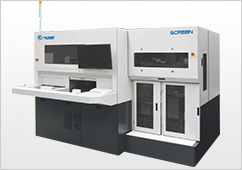
Automatic Optical Inspection System MIYABI 7
In the newly developed lighting unit mounted on MIYABI 7, three types of light sources can be selected, and even substrates hard to secure contrast can be seen, and favorable inspection results can be obtained. Also equipped with newly developed logic for LVH (laser via).
MIYABI 7 detects any abnormalities in PCB hole inspections, such as hole diameter deviation and via bottom failure, up to the LVH of the top diameter 60 μm class in addition to the through hole.
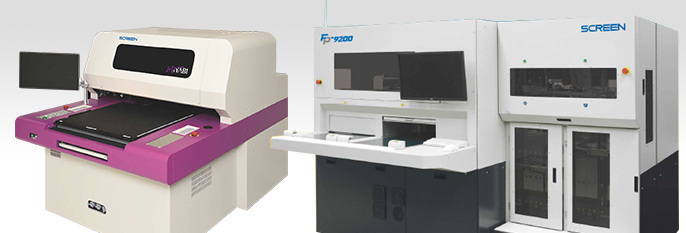
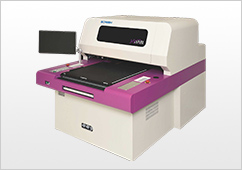
Automatic Final Visual Inspection System FP-9200
A variety of convenient functions are available to accelerate setup procedures. Auto-preparation enables all operations from substrate image scanning to master creation to be automatically set in a single process, while test inspection skips the transfer step for test substrates, allowing repeated inspection. Auto-false call elimination also assists with the adjustment of inspection parameters. Compared to standard systems, the FP-9200 series provides a new level of simplifed, high-speed setup.
Exposure System
Direct Imaging System Ledia 6/6H
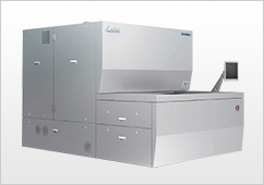
The Ledia direct imaging system continues to deliver the reliable exposure technology needed to meet the growing requirement for a wide variety of printed circuit boards. Ledia is able to supply the increasingly dense, high-precision PCBs required for mobile devices as well as the expanding field of car electronics.
The flexible control enabled by its three wavelength light source provides broader coverage of the wavelength regions for exposure, significantly expanding the number of supported resist types. This format improves productivity by up to 100 percent compared to two wavelength models.
Ledia is also equipped with a proprietary alignment algorithm that compensates for substrate distortion. This function helps to maintain the exceptionally high-definition finish and outstanding throughput direct imaging systems are known for.
Ledia brings together a comprehensive range of cutting-edge technologies for direct imaging that have kept it at the forefront of the industry. If your company is serious about growing its business and profits, Ledia is the partner you need.